What are the characteristics, functions, and applications of MOS transistors?
When designing switch mode power supplies or motor drive circuits using MOS transistors, most people consider factors such as MOS on resistance, maximum voltage, and maximum current, while many people only consider these factors. This type of circuit may work, but it is not excellent and is not allowed as a formal product design.
1. Types and structures of MOS transistors
MOSFET is a type of FET (the other being JFET) that can be manufactured in either enhancement or depletion mode, with a total of four types: P-channel or N-channel. However, in practical applications, only enhancement mode N-channel MOS and enhancement mode P-channel MOS are used, so NMOS or PMOS are usually referred to as these two types.
On the MOS transistor schematic, it can be seen that there is a parasitic diode between the drain and source. This is called a body diode, which is important for driving inductive loads such as motors. By the way, body diodes only exist in individual MOS transistors and are usually not present inside integrated circuit chips. The following diagram is the construction diagram of a MOS transistor, which is usually drawn as shown in the diagram on the right.

2. MOS transistor conduction characteristics
The meaning of conduction is to act as a switch, equivalent to closing the switch.
The characteristic of NMOS is that Vgs will conduct when it is greater than a certain value, which is suitable for use in situations where the source is grounded (low-end driving), as long as the gate voltage reaches 4V or 10V.
The characteristic of PMOS is that Vgs will conduct when it is less than a certain value, which is the case when VCC is connected to the source (high-end drive). However, although PMOS can be conveniently used as a high-end driver, due to its high on resistance, high price, and limited replacement options, NMOS is still commonly used in high-end drivers.
The right figure shows the relationship between Vgs voltage and Vds voltage of Renesas 2SK3418. It can be seen that when the current is low, Vgs reaches 4V, and the voltage drop between DS is already very small, indicating conduction.
3. Loss of MOS switching transistor
Whether it is NMOS or PMOS, there is a conduction resistance after conduction, so while current flows between DS, there is also a voltage at both ends (as shown in the 2SK3418 characteristic diagram), so the current will consume energy on this resistance, and the energy consumed in this part is called conduction loss. Choosing MOS transistors with low on resistance will reduce conduction losses. The current on resistance of low-power MOS transistors is generally around tens of milliohms, and there are also several milliohms.
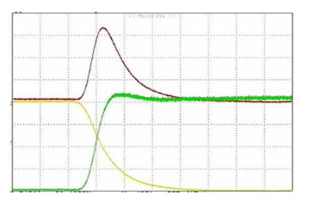
MOS does not complete its conduction and cutoff in an instant. The voltage across the MOS has a decreasing process, and the current flowing through it has an increasing process. During this period, the loss of the MOS transistor is the product of the voltage and current, called the switching loss. Usually, the switching loss is much greater than the conduction loss, and the faster the switching frequency, the greater the loss.
The following figure shows the waveform when the MOS transistor is conducting. It can be seen that the product of the voltage and current at the moment of conduction is very large, resulting in significant losses. Reducing the switching time can reduce the loss during each conduction; Reducing the switching frequency can decrease the number of switches per unit time. Both of these methods can reduce switch losses。

4. MOS transistor application circuit
The most significant characteristic of MOS transistors is their good switching properties, so they are widely used in circuits that require electronic switches, such as switch power supplies and motor drives, as well as lighting dimming
Contact: Emma Tan
Phone: +8613650089053
E-mail: emma@yfwdiode.com
Add: No.9 Cuibi street,Nancheng,Zhang mutou town,Dongguan City,Guangdong Province