
Date:2025-06-20 Categories:Product knowledge Hits:619 From:Guangdong Youfeng Microelectronics Co., Ltd
3.1 BJT Small - Signal Model
Transconductance (gm): Defined as the change in collector current (ΔIC) divided by the change in base - emitter voltage (ΔVBE) in the small - signal regime,gm=ΔVBEΔIC. It represents the transistor's ability to convert a small change in input voltage into a changein output current. For a BJT in the activeregion,gm=VTIC, whereVTis the thermal voltage (VT≈26 mVat room temperature).nput Resistance (rπ): This is the resistance seen at the base - emitterterminals of the BJT in the small - signal model. It is related to the current gainβand the transconductancegmbyrπ=gmβ
.Output Resistance (ro): Represents the resistance seen at the collector - emitter terminals. It is due to the Early effect, which causes the effective base - width to change with the collector - base voltage. A higherrovalue means that the collector current is less affected by changes in the collector - emitter voltage.
Transconductance (gm): For a MOSFET,gmis defined as the change in drain current (ΔID) divided by the change in gate - source voltage (ΔVGS) in the small - signal regime. In the saturation region,
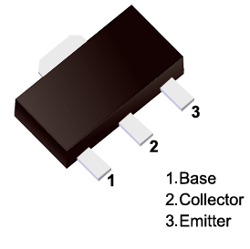
is the threshold voltage. Small-Signal Transistors
Output Resistance (ro): Similar to the BJT, the output resistance of a FET represents the resistance seen at the drain - source terminals. It accounts for the channel - length modulation effect, which causes the drain current to change slightly with the drain - source voltage even in the saturation region. Small-Signal Transistors
Previous: Classification, Structure, and Principle of MOSFET
Next: Renesas tunable antenna varactor diodes for One-Seg broadcasting applications 1
